Adding Bluetooth to a Vintage Radio

I’m writing this as much for my own use as anything else – I keep having to re-invent this solution every time I fix a vintage radio.

Most vintage radios are AM only, and in my part of the world, the only thing on AM is talk radio. Even if that weren’t the case, let’s be honest, most of what people listen to these days is streamed. I don’t like my radios to be shelf-queens, I want to be able to use them and honestly, the sound from the bigger radios is great.

One solution to this is to add an aux-in so that you can plug in an external source and play it through the radio. this certainly works (and you can use most of what is here to do that), but you still need a Bluetooth dongle and leads, and you have to charge it up and turn it on and switch the radio to aux-in. This solution wires the Bluetooth ‘dongle’ into the radio directly, so that it comes on when the radio comes on.

Overview

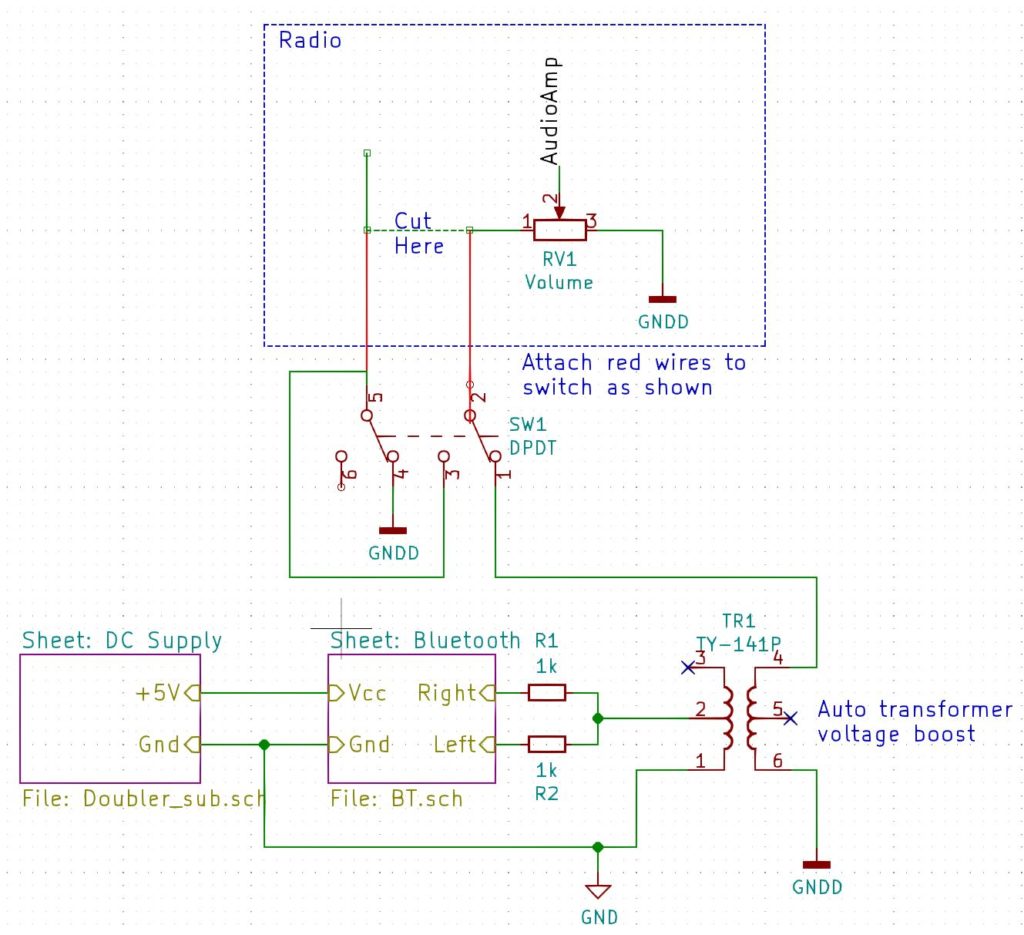
This shows a high-level view of what we are going to do:

Bluetooth Mod Overview

Radio Modifications

Let’s look at the radio block first. The modification here is the same regardless of what external source we are going to wire in. We are going to wire our new audio source across the volume control.

Find the lead going to the volume control that is not connected to ground and does not go to the audio ouput stage. we will cut this wire and route it to a double-pole double-throw switch. A double-pole double-throw switch is simply a switch with two positions (double-throw) that switches two sources at the same time (double-pole). In one position the switch will connect that wire back to the volume control. In the other position it will connect our new audio source instead.

NOTE: It is a good idea to use shielded cable to make the connections between the radio and the switch. Connect the shield to chassis ground.

In the diagram above you can see (hopefully) that when our new audio source is connected, the original one is connected to ground rather than just left floating. This helps stop sound from the RF/IF stages of the radio from bleeding through to the speaker.

Bluetooth Module

The next block to look at as the one marked Bluetooth. You will see that the right and left channels are connected together via two 1k resistors. The use of these resistors prevents the output from one channel destroying the other channel.

Transformer

The next block we will talk about is the auto-transformer. This can serve two purposes.

The first is to boost the output of the Bluetooth module so that it has about the same loudness for a given volume setting as the radio itself. The particular model I am using is the TY-141P. If it is wired as shown in the diagram it gives a 1:2 voltage boost, which seems about right on all the radios I have modded. Triad make another transformer – the TY-142P that can give a boost of 1:2.24 or 1:4.48 depending on how it is wired.

The second purpose is that it can act as an isolation transformer to decouple the new audio source from the radio. This can help to remove ground-loop hum that can arise depending on how the new source is powered. In some scenarios, the chassis ground (GNDD) may be the same as the power supply ground (GND).

NOTE: The point that the auto-transformer is connected to chassis ground can be important. I have found that if you connect it to the volume ground terminal, you will hear hash from the Bluetooth receiver when listening to broadcasts. Experiment with different locations. If all else fails, use a three-pole double-throw switch to disconnect the power to the Bluetooth unit when listening to broadcasts.

Bluetooth Module Details

My preferred Bluetooth module is the KRC-86B, pictured below:

KRC-86B Bluetooth Module

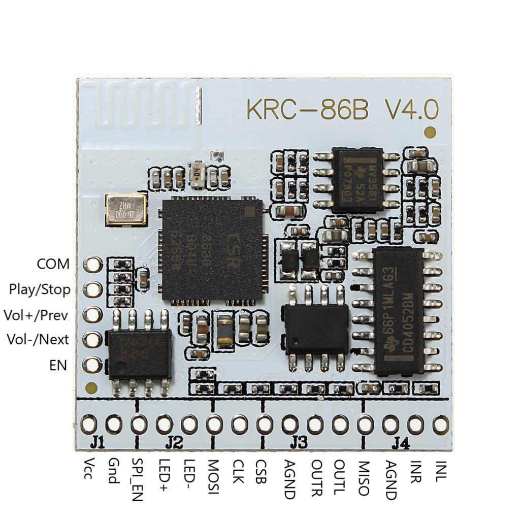
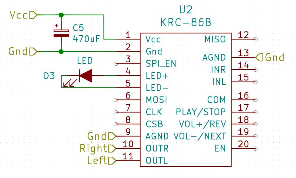
There are a lot of possible connections that we aren’t going to use. We are just going to provide it with a Vcc of +5V and use OUTL and OUTR like so:

KRC-86B Connections

The LED indicates the state of the module. If it is connected it will be steady. If it is not connected it will be flashing, and if there is no power, it will be off! The capacitor is just a decoupling capacitor. Both of these are normally provided with the module.

Power Supply Details

The KRC-86B needs 3.7V to 5V. You could provide this with a battery pack or an external 5V supply and you could wire this power source in to the switch so that it only powered the module when it was selected as an input, but you would need a three-pole double-throw switch to do that.

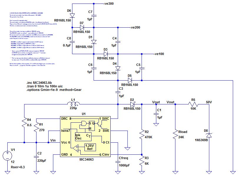
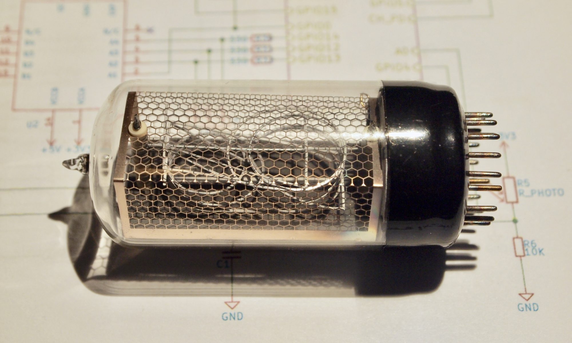
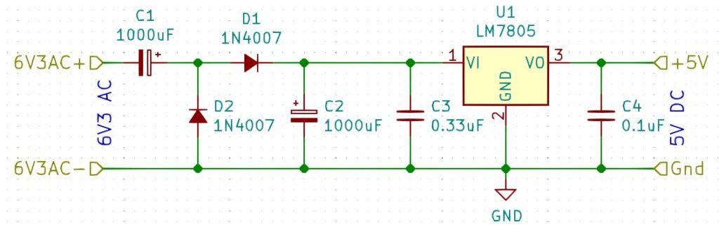
The module only draws at most 80mA, so let’s see if we can provide that directly from the radio. We will probably need to convert some AC voltage into a DC voltage. Some radios have a transformer that provides the filament voltage, and these are probably the cleanest way to power the device. We can just convert the 6.3V AC into 5V DC. Another alternative I have used is to connect my power supply in parallel with the filament of a vacuum tube.

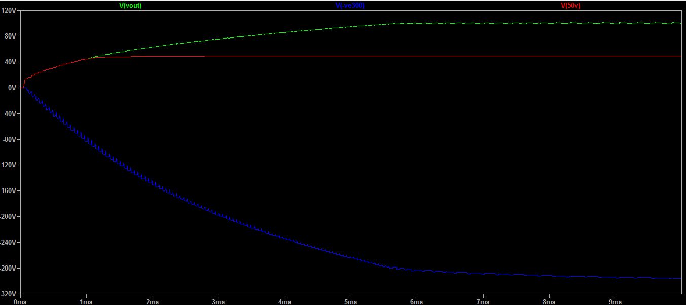
The basic idea is to rectify the AC, smooth it and then feed this through a 5V voltage regulator. 8V-12V is ideal for using a bridge rectifier, however 6.3V won’t provide a high enough rectified and smoothed voltage to feed a 5V voltage regulator, so in this case we need to use a voltage doubler as in the circuit below:

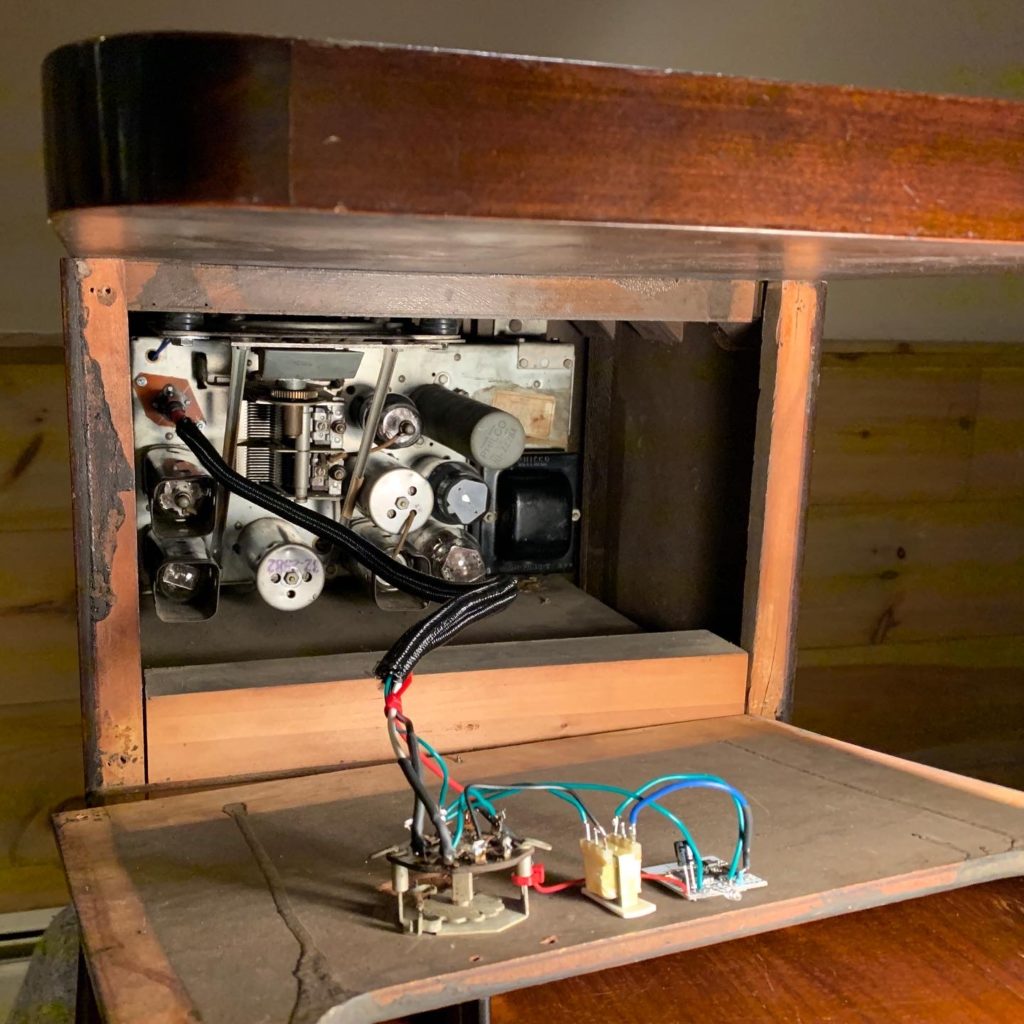
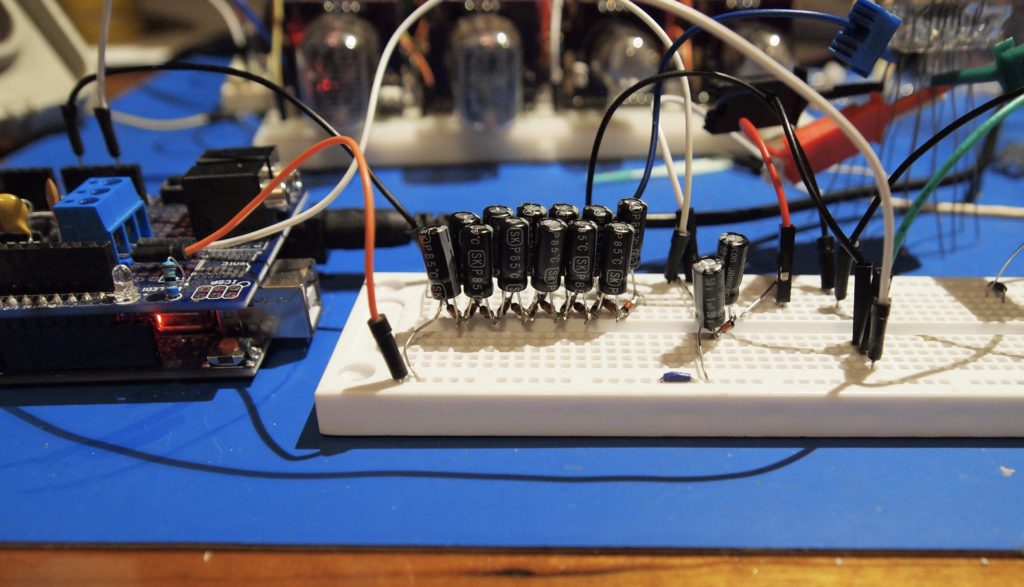
Here’s what it looks like. In this case, there was a handy post I can screw it to:

5V DC Power Supply

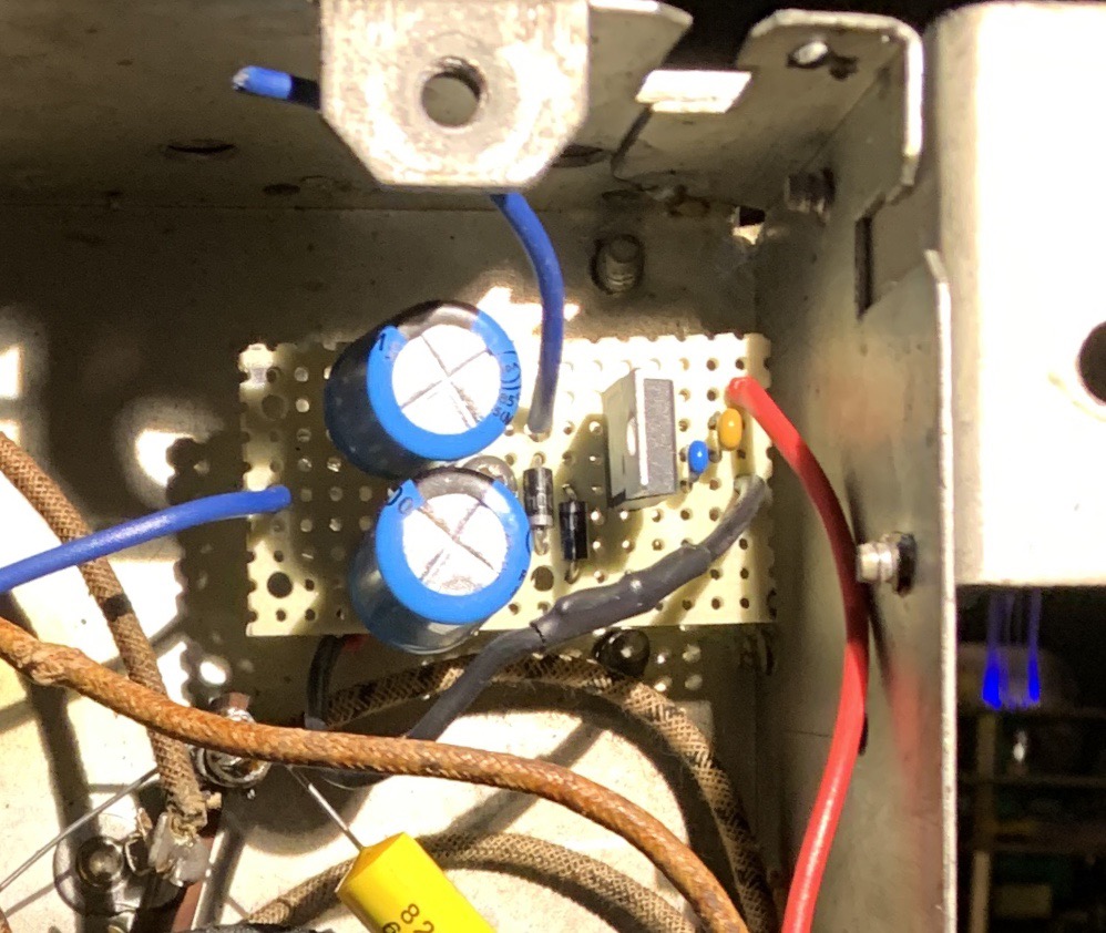
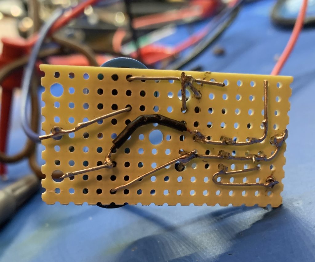
This is what it looks like underneath:

Some nifty point-to-point wiring

Finally, here is what the module, switch and auto-transformer look like in one of the radios I modded. In this case the switch was already there from a mod that had been made in the dim and distant past:

Bluetooth mod installed in a Philco 38-7 chairside radio

Controlling an ITS1A Thyratron

In an earlier post, I explored how to light up an ITS1A Thyratron – this is an old seven-segment display device from the former USSR:

Glowing ITS1A

It requires some exotic voltages: -250V, +40V, +100V and logic-level signals for segment control. A high logic level can be anything between +0.4V and +4V, so a +3.3V device is perfect. The other voltages can be obtained from a 50V boost converter driven with a +5V input. I used Cockroft-Walton ladders to get +100V and -250V and a voltage divider to get the 40V. These are the pins on the tube:

Physical pin descriptions of the ITS1A

This is a description of the pins:

ITS1A pin descriptions

What I didn’t manage to do at the time was figure out how to select which segments get displayed. In my tests, they all lit up. Basically, if the segments are pulled to zero volts, they will be on. If the are raised above +0.4V, they will be off. But only if the other pins are held at the right voltages in the right sequence. Later on I found that I could set the segment voltages, then pull anode one and anode two low for a short period, then high again, then the displayed segments would latch on according to their voltages at the time the anodes were pulled low. The segments will stay that way, regardless of what is done to them, until the anodes are briefly pulled low again.

I suspected that grid two also played a role here, but I was unable to figure it out. Then I came across this archive, which had a circuit diagram and some PIC assembler. In that circuit, the +40V is obtained with a zener which is just connected to ground, with no pull up to keep the voltage at the zener voltage.

(NOTE: This paragraph has been edited from its original). The function of the second grid was revealed looking at the assembler source code. Basically, to set a display you start with the anodes at their set voltages and the second grid above 0.4 volts. Then you briefly pull the anodes to 0V. Then you set the voltages of the segments, then you briefly pull the second grid to 0V (note the line for the second grid below is incorrect, it should be inverted):

Signal sequence for setting the segments of an ITS1A

When the 2nd anode is at 100V, current also flows into the 1st anode (the 40V one) and the zener clamps the voltage to 40V. When the 2nd anode is pulled to 0V, current direction of the 1st anode is reversed, and so it is pulled to 0V too. This is what the datasheet says:

The current of the grids and the 1st anode in the non-conducting state has a positive direction, in the conducting state the direction of the current is changed.

So here is a circuit diagram:

Multiplexed operation of two ITS1A tubes

The tubes are multiplexed by setting the value of the 2nd grid individually for each tube. If the second grid on a specific tube is not pulled above +0.4V, it’s display won’t change. Note that the reset pulse only has to happen once, then you can set the display of all the tubes, one at a time by setting the segment voltages and toggling the 2nd grid on the tube(s) you want to change. Repeat the sequence the next time the display changes.

At first I was slightly annoyed that I had ITS1A tubes, which have a maximum logic level of +4.0V, v. The ITS1B tube has a maximum logic level of +5V. But it is actually a good match for modern controllers, with a +3.3V logic level. I used the trusty Wemos D1 mini Pro to test out the circuit above.

Trials and Tribulations

This was supposed to be a quick build of one of my one-tube-clocks, with a few tweaks to try and improve some of the features. This is what an earlier version looked like:

All my other builds had taken around 3 hours, and the worst that went wrong was a few dry joints. This build was very different:

  1. I had three attempts at getting the solder paste applied – that is three complete wipes and restarts.  It kept smudging, or leaking onto adjacent pads. This was an omen.
  2. Finally I had something I could work with, but I had to touch up some teeny tiny pads on the CP2102N footprint – a QFN28. They were right next to a trace I had cut. I got solder-paste in the cut. I had to get it out, otherwise it would short the two halves of the trace back together. Cue some very fiddly cleaning using a magnifier.
  3. Finally got everything in place, and transferred the board to my hotplate. It was almost cooked and I realized I had forgotten a component, so I had to take it off and let it cool and then add the missing component.
  4. When transferring the board back to the hotplate, I spilled the whole lot on the floor! Fortunately most stayed put, but I had to spend quite a bit of time inspecting things to make sure it was OK, moving some items back into place, and replacing others that had vanished into the carpet.
  5. Second cooking. Looking good.
  6. First test: Plug it into a USB port on my computer. No beeping sound. Nada. I check voltages on the board in a few places, they are all fine, what is going on? I decide to try another device in the same USB port. Nothing. Now this is worrying: had I blown the port? Then I remembered I had the laptop connected to bluetooth audio. The receiver was switched off. So I disconnected bluetooth and plugged my second device into the USB port to check the port, nice noise, port was fine. Now I’m thinking that my new board is probably fine too. Plug that in, no noise. Nada. So, check the soldering. Looks fine, but I touch up the pins on the USB/UART chip that handle the USB connections and now I get the happy sounds from the laptop, so I solder on some indicator LEDs and some connectors.
  7. Next test: Program the ESP8285 on the board. No go. Laptop can’t talk to the ESP8285. I spent quite a while trying to trouble-shoot this. I touched up the pins on the USB/UART chip that interface to the ESP8285. No difference. I wondered if maybe the second cooking had broken the ESP. It looked like there was a blister on it. However I figured I should check some of the signals on the ESP, so I start counting clockwise from pin 1. When I got to the pin that should have been GPIO0, something didn’t seem right. It shouldn’t have been on that side of the board. Then I realized: I had soldered the chip on the wrong way! Arghhhhhh. I was resigned to just salvaging what components I could on the board and throwing it away, but I was tempted to heat the board back up again, pull the ESP and solder a new one on. To do that I would have to unsolder those connectors and LEDs. Not a trivial task. Then it occurred to me: I have a heat gun (not one specific to PCB work, just a regular old heatgun like you might use for stripping paint). I figured I might as well see if I could use it to de-solder the ESP, and amazingly it worked. I fitted a new chip in the right orientation and used the heat gun to solder it. I tried to program it again, and it worked! I can connect to my web server running on the ESP and mess with the controls.
  8. So I plug in a Nixie tube adapter and nothing. Oh come on! I start checking voltages and there is no 5V. 5V is used for two things on this board: Lighting up the LEDs and driving the HV switch. I quickly narrow it down to a dry joint on a diode from the USB power line to my 5V circuit.
  9. OK. Plug in the nixie adapter again and it lights up. We are in business! Wait, though. The LEDs on the adapter aren’t lighting up. This is getting ridiculous (maybe that should be more ridiculous). These aren’t just regular LEDs, they are NeoPixels. I just checked the power above, so I look at the signal lines. They go through a 3V3 to 5V level converter. The signal was non-existant. It was 0V on the 3V3 side and weirdly it was 5V on the 5V side. This is not an inverting level converter, so it should have been 0V too. Except it shouldn’t be 0V at all, it should have a PWM signal on it. I check the connections from the ESP to the level converter, it is all good. There is a pull-up resistor in that line, so something was driving it to zero. All the signals to the HV chip go through the same level converter, and they were working just fine. Finally, though, I decide it has to be the level converter, because 0V should not become 5V. Time to de-solder that chip (another QFN-type package) and replace it.
  10. Plug in the Nixie adapter again, and now I have LEDs. But now the Nixie tube is blank! It has to be the level converter again, so I start tracing signals and yes, I have a dry(ish) joint on one of the pins. I touch that up, plug in the adapter and, finally, everything works.

So, eight hours later and I’m actually quite please that I managed to trouble-shoot this. Plus I learned how to do re-work using a hot air gun (BTW, the gun does have various temperature and ‘ferocity’ settings).

I have yet to clean up though:


ITS1A Power Supply Part II

As I delved more into making a power supply for the ITS1A thyratron, the design became more complex. For example, to produce 100V from the inductor I would need an external FET. To switch the FET properly, I would need another transistor. If I was going to do that, I would use a completely different chip in the first place. So I re-considered what I was trying to achieve, which was simply to light up one of my tubes, just to prove that I could. So I used an existing 50V power supply I had built using the MC34063, and just built two Cockcroft -Walton ladders – a regular voltage doubler for the +100V, and a ridiculous ladder with 12 diodes for the -300V. Actually the data sheet (which I translated with the help of an online OCR and google translate) says that should be -250V. So that is what I used. Here is a picture:

A 6x voltage multiplier

I verified all the voltages, then the next step was to figure out what pins did what. Careful examination of the tube showed that two pins were cut short – this correlated with two pins described as ‘free’ on the data sheet and that allowed me to figure out what went where:

Physical pin descriptions of the ITS1A

Translated description of what the pins are

So with this I was able to wire the tube up and get it to glow:

Glowing ITS1A

You can clearly see the detail of how the phosphor is activated.

What I haven’t been able to do is to control which segments are on an which are off! It is clearly something to do with grid two, but I haven’t been able to figure it out yet.

ITS1A Power Supply

I have been meaning to get some ITS1A thyratron display tubes for some time, and finally bought some a few weeks ago. These are a seven segment display tube that looks a little like a VFD tube when on – they use the same phosphor – but they are driven entirely differently.

An ITS1A on ebay

Although they can be controlled with logic-level signals (roughly 1V to 5V), they require a bizarre set of voltages to actually activate them. The data sheet specifies around 40V, 100V and -240V. Others have apparently driven them with 50V, 100V and -300V. Yes, that’s right, that is minus 300V.

Now I don’t happen to have a power supply lying around that can produce that range of voltages, but it is surprisingly easy to build one. Or at least design one. I haven’t built it yet. The principle is to first build a simple boost converter, then use  a Cockcroft-Walton voltage multiplier driven from the un-rectified output of the inductor, to get the negative voltage. I simulated one in LTSpice. I set the output voltage to 100V. Built a diode/capacitor ladder for the -300V and used a 50V zener diode voltage clamp to create the 50V. This is what it looks like:

A boost converter that will produce the voltages needed to drive an ITS1A

This is what the simulation looks like:

Voltage plots for the boost converter

The part numbers for the diodes are just examples. I haven’t actually chosen them yet. Both the diodes and the capacitors in the ladder need to be able to handle over 100V. The capacitors should be low ESR types. The inductor needs to be able to handle the expected current, though I haven;t figured out what that is yet. However my aim with this is to just be able to test that the tubes work, and maybe have a little fun with them. An actual clock will come later.